Nanofabrication
Our nanofabrication facility offers industry-compatible nanoelectronics/ nanophotonics processing, including 150mm and 200mm wafer capability. Our lithography capability combines photo- and electron beam lithography from 20nm with nano-imprint and hot embossing. Self-assembly of nanostructures is used to grow carbon nanotubes, nanowires and quantum dots. Thin film deposition is performed by ALD or PECVD. We can deposit optical layers using Plasma Assisted Reactive Magnetron Sputtering, and fabricate multi-stack devices using wafer-to-wafer aligning and bonding. We offer device fabrication for silicon electronics, photonics, MEMS, lab-on-a-chip, and spintronics. Fabrication/characterisation capability includes FIB with integrated SEM and SIMS. The range of other measurement tools available include ellipsometry, XPS, Raman spectroscopy, cryogenic prober, RF measurements up to 60GHz, Field-Emission Scanning Electron Microscopy (FESEM), AFMs and a Helium Ion Microscope.
Achievements
A uniquely broad range of technologies, combining traditional and novel top down fabrication with state-of-the-art bottom up fabrication, and extensive characterisation capabilities, including:
- Photolithography and electron beam lithography down to 5nm and very high resolution direct write lithography (~4nm).
- Atomic Layer Deposition of sub-monolayer (>1nm) films with remarkable uniformity and Plasma Assisted Reactive Magnetron Sputtering for deposition of high quality, low loss optical layers.
- Self-assembly fabrication of nanostructures to grow nanowires, nanotubes and quantum dots.
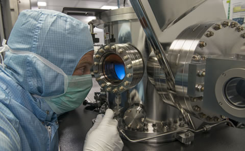
- The ORION™ Helium Ion Microscope provides images of unrivalled high resolution, surface information and material contrast. The microscope has achieved a record 0.24nm resolution and its capabilities are being developed in collaboration with Zeiss.
- Focused Ion Beam - a dual beam with integrated SEM including SIMS, and Field Emission Scanning Electron Microscope (FESEM) which uses a focused and scanned electron beam to produce a magnified image of a sample surface at higher resolutions than a standard SEM.
- Characterisation including raman spectroscopy, cryogenic prober, ellipsometry and RF measurements up to 60Ghz.
Facility contact
Contact us to discuss how you can access our facilities for research and development projects.
University of Southampton staff can find out how to access the facilities by visiting the Zepler Institute Sharepoint.
Equipment
Click to view the Nanofabrication equipment list
Services
Our experts can offer a wide range of fabrication and characterisation services to support your specific requirements. Find out more at: Nanofabrication services